
Investible is proud to announce that we have led Syenta’s $A8.8 million Pre-Series A round through our Early-Stage Fund 2, Climate Tech Fund and Club Investible investment syndicate, alongside a fantastic line-up of investors, including Blackbird, In-Q-Tel, SG Innovate, OIF Ventures, Salus Ventures, Jelix Ventures, Wollemi Capital Group, Brindabella Capital and various angels. This marks Investible’s 50th investment from our Early-Stage Fund 2 and second tripartite investment across 3 of our active investment vehicles!
Syenta is the key technology enabler for the next-generation of AI and HPC chips. A spinout from the ANU, Syenta has developed and patented a novel fabrication process called Localised Electrochemical Manufacturing (LEM) that fabricates micron resolution advanced packaging. Their technology is fundamental to bridging the memory/compute gap, one of the biggest bottlenecks for advancing AI performance. With LEM, Syenta is able to fabricate world-leading elements of advanced packaging, dramatically reduces the number of steps required in traditional advanced packaging, and drive ~60% lower fabrication costs. The process can be scaled up to panel level while maintaining these benefits, to significantly increase the total output, and meet the needs from generative AI.
The Investment Team met the company back in mid-2022 when the company was still called Spark3D and was focused on applications within the photovoltaics industry. Since then, the Syenta team has worked tirelessly to refine their LEM technology, and add talented individuals to the leadership team and Advisory Board. After reconnecting with Syenta in mid-2024, our team was thoroughly impressed by their progress and shift in product focus towards semiconductor advanced packaging.
You can view the process video here at https://www.syenta.com/services-4.
Strong market tailwinds driven by AI and the need for mass manufacturing of high-performance semiconductors
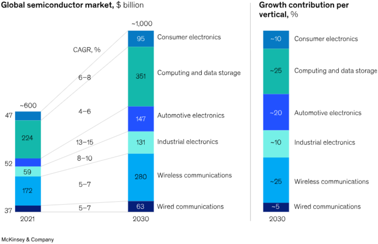
Current semiconductor chip production and performance is unable to keep up with demand for generative AI infrastructure solutions, which require high levels of compute power while balancing cost, energy and speed-to-market considerations.
It is estimated that by 2030, the demand for semiconductor wafers for use in generative AI infrastructure would require an additional 1.2 to 3.6 million wafers to be produced with nodes that are equal to or less than 3 nanometres, which in turn need to be paired with an equivalent amount of advanced packaging wafers. Hence, there is a significant supply gap based on current global foundry fabrication levels, with US$1 trillion in spend into semiconductor foundries expected by 2030, primarily across Asia, the US and Europe.
Additionally, Moore’s law (the observation that the number of transistors in an integrated circuit doubles approximately every 2 years) is starting to reach its limit for 2D chip designs. Hence, there is a need to explore more innovative, faster and cost-effective methods within 2.5D and 3D chip design beyond traditional advanced packaging methods (e.g. photolithography) that can improve resolution size for more effective chip stacking.
Given the early market cycle, Syenta is in a prime position with its intellectual property for LEM to capitalise on these industry tailwinds. Specifically, Syenta’s LEM Technology could be sold directly to foundries and other packaging manufacturers for integration with existing advanced packaging production lines.
Positive partnership interest from the US and reputable semiconductor industry players
Since their visit to the US in mid-2024 for Semicon West and the SelectUSA Tech Program (in which they won 1st place out of 260 participants), Syenta has garnered very positive interest from US-based Government and education authorities, including a significant investment from the Arizona State Government which will be leveraged to help the team continue establishing onshore semiconductor capabilities.
Syenta has already received significant pre-sale commitments for its first Achyon product. Additionally, based on current discussions with numerous blue-chip global semiconductor industry players, research organisations and Government authorities, Syenta have identified over US$15 million in probability-weighted contract value currently sitting in its customer pipeline.
Highly technical founders with deep electronics and materials development experience
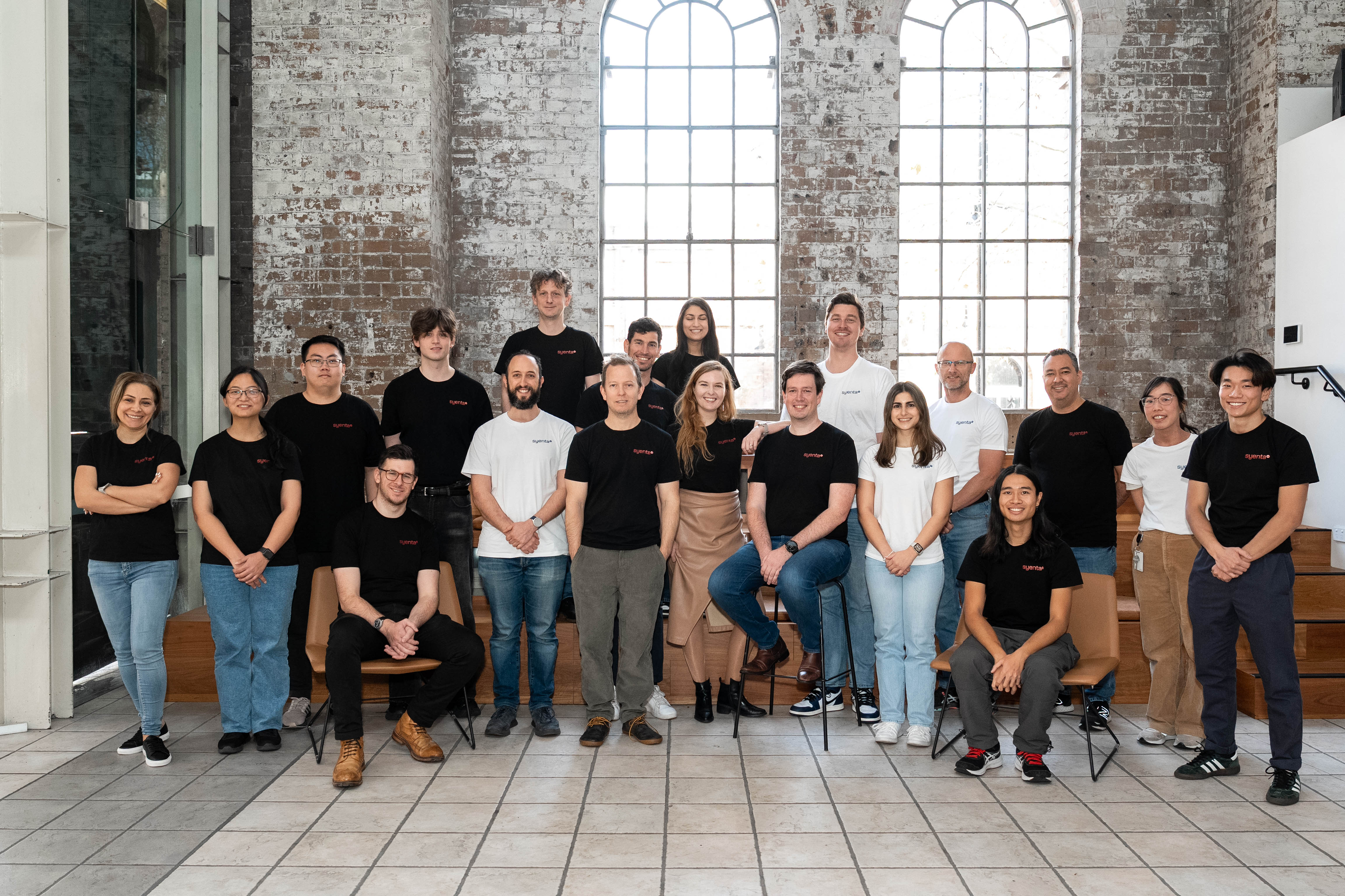
Syenta is led by the ambitious and talented Dr. Jeka Viktorova (CEO), who has over 10 years of experience in chemistry and printed electronics across Europe and Australia, while working at global research institutes and industry. Together with fellow co-founder Professor Luke Connal (CSO), who has over 20 years of experience in materials development , they developed the core intellectual property for LEM and Achyon during Jeka’s PhD at the ANU.
To round out the rest of the founding team, Jeka and Luke eventually brought on Ben Wilkinson (CTO) and Zach Dowse (COO) to bring Syenta’s vision to life. Ben was previously CEO & Co-founder of Rexergy (smart energy market optimisation platform) and with a background in applied physics and photovoltaics metallisation. Zach is a serial founder with a successful exit, previous manager of the Canberra Innovation Network incubator, and neuroscientist (optogenetics).
We couldn’t be more excited to be backing Jeka, Zach, Ben and Luke as they revolutionise the global semiconductor industry and create a new standard for efficiency and sustainability in semiconductor advanced packaging!

Written by
Nicholas Ooi

stay in the loop
The Investible newsletter is your source for our latest news, insights and more
The Investible group of companies includes various entities who are corporate authorised representatives (CAR) of Boutique Capital Pty Ltd (BCPL) AFSL 508011. The full list of entities are detailed here.
CAR has taken all reasonable care in producing all the information contained in the website including but not limited to reports, tables, maps, diagrams and photographs. However, CAR will not be responsible for loss or damage arising from the use of this information. The contents of this website should not be used as a substitute for detailed investigations or analysis on any issues or questions the reader wishes to have answered.
You may download the information for your own personal use or to inform others about our materials, but you may not reproduce or modify it without our express permission. To the extent to which this website contains advice it is general advice only and has been prepared by the Company for individuals identified as wholesale investors for the purposes of providing a financial product or financial service, under Section 761G or Section 761GA of the Corporations Act 2001 (Cth).
The information in this website is not intended to be relied upon as advice to investors or potential investors and has been prepared without taking into account personal investment objectives, financial circumstances or particular needs. Recipients of this information are advised to consult their own professional advisers about legal, tax, financial or other matters relevant to the suitability of this information.
Any investment(s) summarised in this website is subject to known and unknown risks, some of which are beyond the control of CAR and their directors, employees, advisers or agents. CAR does not guarantee any particular rate of return or the performance, nor does CAR and its directors personally guarantee the repayment of capital or any particular tax treatment. Past performance is not indicative of future performance.
All investments carry some level of risk, and there is typically a direct relationship between risk and return. We describe what steps we take to mitigate risk (where possible) in the investment documentation, which must be read prior to investing. It is important to note risk cannot be mitigated completely.
Whilst the contents of this website is based on information from sources which CAR considers reliable, its accuracy and completeness cannot be guaranteed. Data is not necessarily audited or independently verified. Any opinions reflect CAR’s judgment at this date and are subject to change. CAR has no obligation to provide revised assessments in the event of changed circumstances. To the extent permitted by law, BCPL, CAR and their directors and employees do not accept any liability for the results of any actions taken or not taken on the basis of information in this website, or for any negligent misstatements, errors or omissions.
Subscribe to our newsletter
Be the first to receive the latest news, insights and resources from Investible